Kevin A. Wepasnick, Ph.D., joined the Anderson Materials Evaluation staff as a scientific project manager in July. His prior experience at The Johns Hopkins University was extensive and is summarized in his brief biography below:
Dr. Wepasnick recently joined the staff of AME after completing his Ph.D. dissertation work at The Johns Hopkins University (JHU) in surface chemistry. There, he focused his research on the surface analysis of functionalized and modified carbonaceous nanomaterials and metal nanoparticles. Primarily tasked with understanding the chemical effects of oxidants on carbon nanotubes, he worked on derivatization methods to label specific functional groups on their surfaces to improve quantitative x-ray photoelectron spectroscopy (XPS) analysis of oxidation effects. Beyond XPS, Dr. Wepasnick applied a wide range of characterization techniques to explore the surface chemical and morphological effects of oxidation, including FTIR, TEM, Raman, Auger, AFM, and STM. He also was responsible for running and maintaining the on-campus surface analysis laboratory. In this capacity, he interfaced with over twenty independent research groups from across the JHU system, from outside universities, and from industry. The JHU system includes The John Hopkins Applied Physics Laboratory and Johns Hopkins Medical, a $5 billion medical organization more heavily funded for medical research than any other university hospital system in the United States. He has experience working with a wide range of materials including biomedical materials, metal and metal oxide particles, self-assembled monolayers, CVD process films, and nanoparticles of various phases and compositions. He enjoys using a multitude of analytical techniques to characterize materials and to solve materials problems.
Dr. Lorrie A. Krebs and I are delighted to have him on board with us. His knowledge, versatility, and enthusiasm have immediately made him invaluable to our materials characterization and failure analysis missions.
22 November 2011
02 May 2011
Activated Carbon Website Uses AME SEM Images
A new website for activated carbon has used the activated carbon SEM images from our website used as an illustrative example of our SEM analyses. These images were made by Dr. Lorrie Krebs. The Australian website using these images has done so with our permission. That website is here and uses the images to show the high surface area of activated charcoal. The example from our website is given below:
Illustrative Example 2: Activated Carbon
Figure 1 is a low magnification (50X) SEM micrograph of activated carbon particles of an air filter. Activated carbon is similar to graphitic carbon except that it has a high degree of porosity and a large internal surface area. Activated carbon is mostly used as a filter material for removing impurities from water and various gases. Figure 2 is a moderately magnified (1000X) SEM micrograph (of the particle to the right in Figure 1) indicating internal surfaces and porosity in the activated carbon. This sample was sufficiently conductive that it was not coated.
 | |
Figure 1  Figure 2 |
04 April 2011
Examining a High Intensity Electron Gun Used Cathode with Optical Microscopy
We make it a habit to examine samples sent to us with optical microscopy even if the requested analysis is x-ray photoelectron spectroscopy (XPS), thermal analysis, electrochemistry, or FTIR spectroscopy. While optical microscopy is not the newest of laboratory techniques, it provides relatively easily obtained valuable information. It allows us to document the appearance of a sample so that other materials characterization results can be matched with certain material appearances over time. The next similar sample sent by a customer for analysis may not be as similar as thought. One of most frequent things we learn is whether there are two or more chemical or structural phases present. There may be phases present which optical microscopy will not reveal, but it does very often make it clear that multiple phases are present which the eye may not have perceived or perceived in such detail. This is very important to know when interpreting the quantitative elemental composition determined by XPS or EDX (Energy Dispersive X-ray analysis) or various phase change features in a thermogravimetry, differential scanning calorimetry (DSC), or thermomechanical analysis.
In the optical microscopy images below, we will examine a cathode which has seen 25 months of service in a high intensity electron gun used in an x-ray source. This tungsten cathode consists of a thin circular foil mounted on three legs and doped with cesium to lower its work function. A filament consisting of a serpentine etched circular tungsten foil sits behind it and produces a flood of electrons which are accelerated at 12 KeV into the back side of this cathode. The most common failure mode is that the tungsten filament separates at a grain boundary between grains, which often grow with usage until a single grain traverses the entire current path and the grain boundaries become the strong electron scatterers or the high resistance points until failure occurs at a grain boundary. Another failure mode has been that one of the spot welds holding the three legs of the cathode fails and the cathode shorts out to the extractor lens of the electron gun. In the case of this cathode/filament assembly, the failure was the rupture of the filament.
The cathode shown below was imaged with an inspection microscope with illumination at an angle of about 30 degrees relative to the surface normal. This provides an image much like what the eye sees commonly, though at a much lower magnification.

This surface is highly reflective, so much of the detail is lost. But, we do get a sense that many irregularities and perhaps chemical phases or surface roughness result mostly near the three legs of the cathode. If we place the illuminating light at an angle of about 65 degrees to the surface normal, we get a better image which makes it clear that there is great variability of surface condition on this used cathode. These are also very much enlarged grains with usage etched grain boundaries.

Looking at the cathode at higher magnification we see striation patterns more clearly:

Are these bright lines due to chemical phases or are they ridge lines of raised surface areas? Let us make use of the metallographic microscope with light normal to the surface of the cathode.

This microscope does not offer the depth of field of the inspection microscope, so we cannot see the three legs of the cathode any more. But, we do see that there is a great variation in surface reflectivity and this may create a great variability in local surface electron emission in use. We can make use of a Nomarski interference phase contrast feature of this microscope to differentiate areas of about the same surface height from those of different heights. This mode inserts a prism at the objective lens and uses two polarized films to create images similar to those below:

The areas of a given color are at the same distance from the objective lens, so we can learn more about the surface topography now. If the material being imaged were partially transparent to visible light, we would have to be prepared for possible phase contrast due to materials of different index of refraction, which would probably be due to different chemical phases. This tungsten is to reflective for that to be of concern here. The presence of the colored patterns over a given grain do mean that there is surface topography on that grain. Let us look at a higher magnification at parts of this cathode surface:


At twice the prior magnification:


The upper image of these last two was a relatively non-reflective area near a leg and the very surface rough grain in the lower left corner of the lower image was also near a leg. Note the very wide grain boundary on the right side of the large blue-green grain in the lower image also. Such a wide grain boundary in the filament would likely become a point of separation and failure. The surface roughening is probably due to one of these reasons:
Nomarski phase contrast interference sure can produce some colorful and beautiful images! They are also useful.
In the optical microscopy images below, we will examine a cathode which has seen 25 months of service in a high intensity electron gun used in an x-ray source. This tungsten cathode consists of a thin circular foil mounted on three legs and doped with cesium to lower its work function. A filament consisting of a serpentine etched circular tungsten foil sits behind it and produces a flood of electrons which are accelerated at 12 KeV into the back side of this cathode. The most common failure mode is that the tungsten filament separates at a grain boundary between grains, which often grow with usage until a single grain traverses the entire current path and the grain boundaries become the strong electron scatterers or the high resistance points until failure occurs at a grain boundary. Another failure mode has been that one of the spot welds holding the three legs of the cathode fails and the cathode shorts out to the extractor lens of the electron gun. In the case of this cathode/filament assembly, the failure was the rupture of the filament.
The cathode shown below was imaged with an inspection microscope with illumination at an angle of about 30 degrees relative to the surface normal. This provides an image much like what the eye sees commonly, though at a much lower magnification.

This surface is highly reflective, so much of the detail is lost. But, we do get a sense that many irregularities and perhaps chemical phases or surface roughness result mostly near the three legs of the cathode. If we place the illuminating light at an angle of about 65 degrees to the surface normal, we get a better image which makes it clear that there is great variability of surface condition on this used cathode. These are also very much enlarged grains with usage etched grain boundaries.

Looking at the cathode at higher magnification we see striation patterns more clearly:

Are these bright lines due to chemical phases or are they ridge lines of raised surface areas? Let us make use of the metallographic microscope with light normal to the surface of the cathode.

This microscope does not offer the depth of field of the inspection microscope, so we cannot see the three legs of the cathode any more. But, we do see that there is a great variation in surface reflectivity and this may create a great variability in local surface electron emission in use. We can make use of a Nomarski interference phase contrast feature of this microscope to differentiate areas of about the same surface height from those of different heights. This mode inserts a prism at the objective lens and uses two polarized films to create images similar to those below:

The areas of a given color are at the same distance from the objective lens, so we can learn more about the surface topography now. If the material being imaged were partially transparent to visible light, we would have to be prepared for possible phase contrast due to materials of different index of refraction, which would probably be due to different chemical phases. This tungsten is to reflective for that to be of concern here. The presence of the colored patterns over a given grain do mean that there is surface topography on that grain. Let us look at a higher magnification at parts of this cathode surface:


At twice the prior magnification:


The upper image of these last two was a relatively non-reflective area near a leg and the very surface rough grain in the lower left corner of the lower image was also near a leg. Note the very wide grain boundary on the right side of the large blue-green grain in the lower image also. Such a wide grain boundary in the filament would likely become a point of separation and failure. The surface roughening is probably due to one of these reasons:
- Impurities from the cooler legs migrate to the cathode surface near them and promote the surface ridge lines and other roughened topography.
- Grains near the legs are slightly cooler and impurities incident upon the surface have a higher probability of sticking on the surface and promote surface roughening.
- The surface roughening is a function of a certain range of temperatures due to a phase change of the tungsten crystal structure which occurs in a certain temperature window. Tungsten is usually said to have the bodied centered cubic (bcc), which is its thermodynamically stable phase. It also has a beta phase of simple cubic structure which grows as rods under oblique incidence sputtering of tungsten onto a substrate. Perhaps some impurities may stabilize the simple cubic structure within a certain temperature window.
Nomarski phase contrast interference sure can produce some colorful and beautiful images! They are also useful.
03 April 2011
Move to a Larger and Improved Laboratory Facility
In mid-February 2011, we moved from our old laboratory of 3,592 square feet into our new Columbia, Maryland laboratory of 5,439 square feet in a facility less than 1 mile away from our old laboratory. While our old laboratory was largely taken as was from a prior medical services laboratory, we were able to design the layout of our new laboratory to better suit our needs. We have added an area suitable for environmental and corrosion testing of materials, where it is well-separated from the laboratories we need to keep clean. We have further lab areas suitable for future expanded capabilities. Our laboratory bench and cabinetry space has increased, so we can keep more laboratory tools and implements out and readily available.
Within 1 week of our move, we had all of our spectrometers and microscopes and our thermal analysis instruments up and running again, with the exception of our EDX. We replaced our EDX x-ray detector crystal with one having better carbon and oxygen resolution and detection than our old crystal had provided. Fortunately, work has been pouring in since our move, since we have some very significant liabilities to pay as a result of this move! Lorrie A. Krebs, Ph.D., Stephanie J. Roberg, M.S., and Charles R. Anderson, Ph.D. are eager to talk to you about how we can help you solve your materials characterization, development, processing, failure analysis, and quality control problems and create new materials usage opportunities for you. Our contact information is given in the sidebar, including our e-mail addresses. Feel free to talk to Dr. Lorrie Krebs about your corrosion, electrochemistry, metallography, and fracture failure analysis needs. Talk to Stephanie Roberg about FTIR infra-red spectroscopy requirements and thermal analysis by thermogravimetry (TG or TGA), differential scanning calorimetry (DSC), or thermomechanical analysis (TMA). Finally, discuss surface quantitative elemental and chemical analysis, adhesive bonding problems, and general multi-technique analysis projects with Dr. Charles Anderson.
Those of our clients who are local, please feel free to visit our new laboratory and office facility. Or if you come by to drop off samples or to discuss a materials problem, please feel free to request a tour of the labs.
Our new XPS Surface Analysis Laboratory:

Our new SEM/EDX Laboratory:

Our new FTIR Infra-Red Spectroscopy Laboratory:

Our new Thermal Analysis Laboratory:
Our new Electrochemistry and Corrosion Evaluation Laboratory:

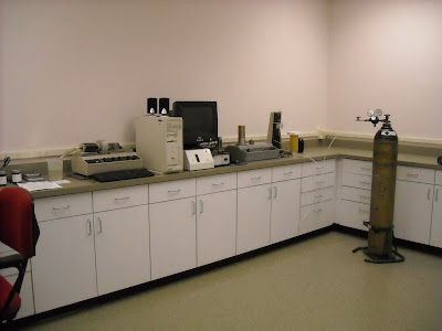
Our new Optical and Metallographic Microscopy Laboratory:

Within 1 week of our move, we had all of our spectrometers and microscopes and our thermal analysis instruments up and running again, with the exception of our EDX. We replaced our EDX x-ray detector crystal with one having better carbon and oxygen resolution and detection than our old crystal had provided. Fortunately, work has been pouring in since our move, since we have some very significant liabilities to pay as a result of this move! Lorrie A. Krebs, Ph.D., Stephanie J. Roberg, M.S., and Charles R. Anderson, Ph.D. are eager to talk to you about how we can help you solve your materials characterization, development, processing, failure analysis, and quality control problems and create new materials usage opportunities for you. Our contact information is given in the sidebar, including our e-mail addresses. Feel free to talk to Dr. Lorrie Krebs about your corrosion, electrochemistry, metallography, and fracture failure analysis needs. Talk to Stephanie Roberg about FTIR infra-red spectroscopy requirements and thermal analysis by thermogravimetry (TG or TGA), differential scanning calorimetry (DSC), or thermomechanical analysis (TMA). Finally, discuss surface quantitative elemental and chemical analysis, adhesive bonding problems, and general multi-technique analysis projects with Dr. Charles Anderson.
Those of our clients who are local, please feel free to visit our new laboratory and office facility. Or if you come by to drop off samples or to discuss a materials problem, please feel free to request a tour of the labs.
Our new XPS Surface Analysis Laboratory:

Our new SEM/EDX Laboratory:

Our new FTIR Infra-Red Spectroscopy Laboratory:

Our new Thermal Analysis Laboratory:

Our new Electrochemistry and Corrosion Evaluation Laboratory:

Our new Optical and Metallographic Microscopy Laboratory:

Subscribe to:
Posts (Atom)